
I’m working on a project that might become a TAPR product Real Soon Now. While almost all its parts are very ordinary, one is unique (and can be expensive) — a u-blox GNSS (global navigation satellite system) module. These come in at least three form factors. Two of them can be hand soldered with care, but most interesting to me are the ZED-F9T and ZED-F9P dual-frequency high performance modules, and the ZED footprint poses some challenges.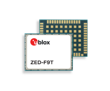 You can see from the picture that unlike some other u-blox devices, the pads aren’t accessible from the side — you can’t get to them with a soldering iron, and the only option is to reflow solder them.
DIY surface mount assembly has become relatively common, and isn’t as difficult as many people think. Solder paste is spread onto the board’s pads using a metal stencil and a squeegee, then the parts are placed on the pads, and finally the whole board is heated to melt the paste into liquid solder. Here’s an old but very good tutorial on SMD soldering using a stencil from the good folks at SparkFun.
Placing all those tiny parts by hand can be really tedious. PCB assembly houses like JLCPCB now offer automated surface mount assembly services for incredibly low prices. JLCPCB stocks all the parts my project uses, except the u-blox module.[1]Actually, they can source those too, but there are drawbacks, but that’s a story for a different post. And having all those parts mounted costs only a couple of dollars per board.
Normally all the SMT parts on the board are soldered in one pass because the stencil holes are just big enough for the solder pads, and won’t fit over components already on the board. It’s possible to use solder paste without a stencil, but it’s really difficult to do cleanly.
So that ruins the idea of having JLCPCB do most of the work, leaving me just the u-blox module to deal with. Or does it?
I’ve found a simple workaround:[2]I don’t claim it’s original to me; I’m sure others have done the same thing. make a stencil with cutouts large enough to clear the mounted parts, while leaving the cutouts for the not-yet-soldered pads alone. Then the stencil will drop over the parts and you can paste, place, and reflow the new components. (I told you it was simple!)
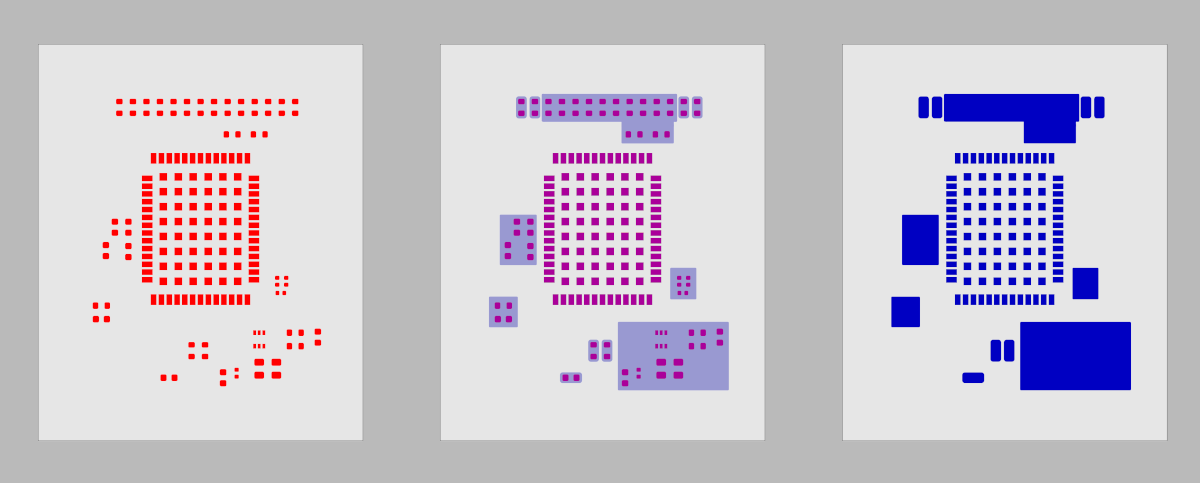 The left image (red) is the original stencil outline. Each of the red spots is a cutout that matches the size of the solder pad below. The big block of pads near the center is the ZED-F9 module. The middle image shows that the cutouts can be enlarged to make openings around the existing parts. The right image (blue) is the new paste layer after editing in cutouts for all the other components.
To modify the stencil in KiCad, open the board file in the PCB Editor and uncheck all layers (tab on right side) except “F.Paste”, “F.Courtyard”, and “Edge.Cuts” (which provides the board dimensions). On the “Objects” tab, make sure “Zones” is checked. You should also click the box on the left side of the screen to “Show filled areas of zones”.
Set F.Paste as the active layer, and use the “Add a Filled Zone” tool to draw boxes over the courtyard for each already-mounted part. There’s no harm in making the zones slightly larger than that. You can include several closely spaced components within a single zone. Try to keep the zone edges as far from the remaining pads as you can. It will make spreading the paste easier. Notice that I kept separate outlines for a few components rather than including them in a large cutout. These cutouts serve as guides to approximately align the stencil on the board and keep it from sliding around.
When you’re finished, do File/Plot/Gerber. Make sure the box “Plot Edge.Cuts on all layers” is checked. Generate the gerber files and send the F_paste.gbr file to the PCB house to get a stencil.
The picture below shows the stencil in action. Scrap boards form a frame to secure the work PCB tightly in place, and everything is securely taped. Make sure the stencil is as flat as possible against the board to keep paste from wicking underneath and making a mess. I arrange the tape so I can hinge the stencil up without smearing the paste.
 I use an infrared preheater. My process isn’t scientific — I keep an eye on the board and once the paste melts and the existing solder reflows I maintain the heat for two or three minutes, then cool the board down gradually to reduce thermal stress. I don’t know if I’m getting anything like the correct thermal profile, but so far all the modules I’ve placed this way have worked.
By the way, my theory is that using a hotplate rather than an oven or hot air gun is better for the health of the u-blox module, which has its own soldered components inside. Heating from below causes the solder on the bottom to flow first, minimizing the heat in the module above.
It took me a long time to find this simple way to assemble these boards without major headaches. This idea has worked well and saved many hours of placing tiny parts with tweezers. I hope you find it useful, too.
References
3 comments
Good that you knew that there are internally soldered components in the module! Look forward to reading more about this new project/ product.
Thanks, Steve! Here’s a link to a pic of the inside of a ZED-F9T. Don’t ask me how I got to see it…
https://www.febo.com/pages/misc/zed_f9t_topless_scaled.jpg
Hi John,
I very much appreciate your work. I used to be an MRI console designer for Varian/Agilent. Now do some consulting with UMINN and MIT. There is another guy with the same unusual name as me out there who is an FPGA guy who was also in the military just in case you look me up. Twice that guy lived in the same city as me. The first time was in Durham NC and he picked up my laundry at the cleaners. The second time in Alameda CA. At one point I was quite concerned with close-in phase noise which is important in NMR (more than MRI). Persistent cryomagnets have phase noise as well as a gradual decline in frequency. Anyway thanks for an interesting website.